- Research
- Open access
- Published:
Cost-effective multi-standard video transform core using time-sharing architecture
EURASIP Journal on Advances in Signal Processing volume 2019, Article number: 49 (2019)
Abstract
This paper presents a cost-effective two-dimensional (2-D) inverse discrete cosine transform (IDCT) for supporting multiple standards of MPEG 1/2/4, H.264, VC-1, and HEVC. The proposed approach employs a time allocation scheme to enable the simultaneous processing of the first and second dimensions in order to enhance data throughput and attain hardware utilization of 100%. The proposed one-dimensional (1-D) IDCT uses distributed arithmetic (DA) in conjunction with factor sharing (FS) within a hardware sharing architecture. Four parallel computation streams are employed to enhance the throughput rate as four times of operation frequency. The efficacy of this approach was verified by fabricating a test chip using the Taiwan Semiconductor Manufacturing Company Limited (TSMC) 90 nm Complementary Metal-Oxide-Semiconductor (CMOS) process. The inverse transform core has an operating frequency of 200 MHz and a throughput of 800 M-pels/s with a gate count of 27.2 K.
1 Introduction
Video compression is used to reduce redundancy in video-related information in order to increase storage capacity and transmission rates. The inverse discrete cosine transform (IDCT) is an application used in video decompression applications to obtain the initial picture. A variety of transform dimensions and coefficients have been developed by the International Organization for Standardization [1], the International Telecommunication Union Telecommunication Standardization Sector [2, 3], and Microsoft Corporation [4].
Numerous transform architectures supporting single standards have been developed to reduce hardware costs [5–7]. The architecture for the Video Codec 1 (VC-1) standard uses matrix decomposition, additions, and row/column permutations to reduce hardware costs [5]. The two-dimensional (2-D) forward and inverse discrete cosine transform (DCT and IDCT) use a single 1-D transform core and a transpose memory with time division to enhance area-efficiency and achieve high-throughput rates for the MPEG standard [6]. High Efficiency Video Coding (HEVC) is the most recent video coding standard, presented in [7]. This architecture uses an efficient constant matrix multiplication scheme implemented in HEVC for DCT. As outlined in [5–7], high area-efficiency and high-throughput rates can be achieved using these architectures to support single standard; however, this approach is unable to match various transforms supporting different standards that designed to support a single standard.
The parallel structure illustrated in Fig. 1a supports multiple standards and hardware sharing schemes outlined in [8–11]: This includes multiple one-dimensional (1-D) fast inverse transform algorithms using sparse matrix decomposition and shift-and-add computation [8, 9]. The common sharing distributed arithmetic (CSDA) algorithm combines factor sharing (FS) and distributed arithmetic (DA) sharing techniques with in the DCT transform presented in [10]. The parallel structure in Fig. 1a combines two similar 1-D transform cores with a single transpose memory with parallel-input parallel-output to achieve high throughput rates. Unfortunately, a parallel structure imposes high hardware costs. This has led to the development of multiplex structures, such as that presented Fig. 1b, comprising single 1-D transform core, a transpose memory, and a multiplexer [12–14]. The two-dimensional (2-D) IDCT in [12] comprises a single 1-D IDCT core, a multiplexer to control the operation of the first-dimensional (1st-D) or second-dimensional (2nd-D) transform and a transpose memory. The architecture in [13] uses a delta coefficient matrix with resource sharing to perform a variety of DCT-based transforms with support for multiple standards. The technique in [14] integrates four 4×4 and two 8×8 transforms using an extended transform and block multiplication. Multiplex structures enable a reduction in hardware cost; however, this approach can compromise overall throughput due to the fact that the 1st-D and 2nd-D operations are performed separately.

Three different structures of 2-D IDCT transform. a Parallel structure. b Multiplex structure. c Simultaneous structure
With the aim of enhancing-throughput and achieving hardware utilization of 100%, we developed a 2-D IDCT comprising a single 1-D IDCT with a transpose memory (TMEM) circuit, as shown in Fig. 1c. The resulting design provides four computation paths in conjunction with a time allocation scheme to enable the simultaneous processing of the 1st-D and 2nd-D. The proposed 1-D IDCT core employs a CSDA algorithm to reduce hardware cost for supporting multiple standards (MPEG 1/2/4, H.264, and VC-1, optional for HEVC). The proposed design provides four computation paths for the IDCT through the implementation of a time allocation scheme, which provides high throughput at low cost as well as support for multiple standards. The 2-D IDCT core presented in this study includes the following features:
The remainder of this paper is organized as follows. In Section 2, we present the mathematical derivation of 2-D IDCT transform and the proposed architecture using time-allocation scheme. A comparison of synthesis results and very-large-scale integration (VLSI) implementation is outlined in Section 3, and conclusions are drawn in Section 4.
2 Method
2.1 Mathematical derivation of 2-D IDCT transform
The 2-D IDCT can be expressed in matrix notation as two 1-D IDCTs. Consider the 1-D IDCT, the inner product for general matrix multiplication is written as
2.1.1 8-point IDCT transform algorithm
In this subsection, we introduce the proposed 8-point inverse transform, which is defined as follows:
where
The MPEG, H.264, VC-1, and HEVC standards use the same 8-point coefficient structure; therefore, the 8-point transform used for these standards can be obtained via the same mathematical derivation. The symmetry of the IDCT coefficient makes it possible for the 1-D 8-point IDCT in (1) to be expressed as (4) and divided into an even part ze and an odd part zo, as listed in (5) and (6), respectively:
where ze and zo can be expressed as
Even part ze can be further decomposed into even part zee and odd part zeo:
where zee and zeo are expressed as
The even part of zee and zeo in (8) and (9) can be expressed as follows:
Odd part zo in (6) can also be expressed as follows:
Using (6) and (8)-(9), the even and odd portions of the output transform can be calculated separately. If the even input data of 1-D IDCT is calculated using an even circuit, then the odd input data of 2-D IDCT can be calculated simultaneously using an odd circuit, which enables the sharing of hardware resources simply by reordering the architecture.
2.1.2 4-point IDCT transform algorithm
The 1D H.264, VC-1, and HEVC 4-point integer is defined as follows:
where
Similar to the even part of 8-point transform in (5), 1-D 4-point standards can be derived using the format presented in (8) and (9). This enables the sharing of hardware resources in H.264/VC-1/HEVC 8-point and 4-point integer transforms. According to (13), the throughput of a 4-point transform is a half that of an 8-point transform. To maintain the same throughput in 4-point and 8-point transforms, we enabled support for the simultaneous processing of data related to two 4×4 matrices for H.264/VC-1 4×4 and VC-1 4×8/8×4 standards. Thus, the input data X4 in (13) includes data for two 4×4 matrices, which necessitates the inclusion of circuits with a symmetrical architecture for the computation of even and odd parts, thereby enabling the simultaneous computation of two input 4×4 matrices based on 4-point standards. Under these conditions, the same throughput can be obtained using the 4-point or 8-point transforms.
2.2 Proposed architecture using time allocation scheme
As shown in Fig. 2, the proposed 2-D IDCT architecture core was implemented using a single 1-D IDCT transform core with one transposed circuit. The 1-D IDCT core includes three reorders, each of which includes two 8-input-4-output multiplexers used to differentiate even and odd part transforms. Even common sharing distributed arithmetic (ECSA) and odd common sharing distributed arithmetic (OCSA) compute data related to the even and odd part transforms of IDCT in order to enable CSDA-based computation. In the even part circuit, ECSA used to compute the addition and subtraction results associated with the even data, as in (8) and (9). Furthermore, four 2-input multiplexers are used for the selection of either 8-point or 4-point transform standards. The multi-dual mode computation (MDMC) circuit comprises four 2-input modified butterfly circuits for addition and subtraction computations using even and odd part data, as in (4). The proposed architecture includes three pipeline stages for the even part circuit and odd part circuits to enable high speed computation. The architecture of the 2-D IDCT transform core and time allocation scheme are detailed in the following.

Proposed 2-D IDCT architecture
2.2.1 Architecture of the 2-D IDCT core
-
1.
Reorder: We implemented a reorder circuit comprising two 8-input-4-output multiplexers for the separation of the two dimensions of the transform in order to enable simultaneous computation. For example, in Reorder 1, when the selected signal is zero (S1=0), even part input data X in the first dimension of the transform are fed into ECSA and odd part data of the second dimension are fed into OCSA. Similarly, when the selected signal is one (S1=1), the odd part input data X are fed into the OCSA for the 1-D transform and the even part of feedback data z2D are fed into ECSA for the 2-D transform. The two dimensions of the transform can be computed simultaneously, which means that the hardware resources can be shared via time-allocation, thereby reducing area overhead and achieving 100% hardware utilization.
-
2.
ECSA and OCSA: In the 1-D transform, the calculation of the even and odd parts can be respectively performed using ECSA and OCSA, both of which are based on CSDA architecture. Mode selected signals Modee in the ECSA and Modeo in the OCSA modules are used to select standards based on Table 1. As shown in Fig. 2, Gee0 and Gee1 are the results of data distribution in the ECSA module. As in (10) and (11), outputs of ECSA modules zee and zeo comprise two coefficient vectors, \(\left [ \begin {array}{cc} c_{4} & c_{4} \end {array} \right ] \) and \(\left [ \begin {array}{cc} c_{2} & c_{6} \end {array} \right ] \), respectively. The transform outputs of zee and zeo require only two adders, two subtractors, a distributed data module, and an even adder-tree (EAT) to obtain output results. Data distribution modules are used to assign various non-zero values for each weight, whereupon the EAT sums them up to complete the transform \(\left [ \begin {array}{cccc} z_{ee1} & z_{ee2} & z_{eo1} & z_{eo2} \end {array} \right ]\). The result is then fed into the even butterfly module to calculate even result ze, as in (7). The even butterfly module is combined with two adders, two subtractors, and four multiplexers, which are used to select either the 8-point or 4-point transform. The odd part transform in (12) can be implemented in the OCSA module using CSDA-based computation using two adders, four subtractors, and an OAT. To maintain the same throughput in the 4-point and 8-point transforms, ECSA and OCSA can be designed as symmetrical circuits based on the fact that the input matrix comprises data from two input matrices in VC-1/H.264 4×4 and VC-1 4×8/8×4 standards. Moreover, the ECSA and OCSA modules are both provided pipelines before the outputs to enable high-speed computation. The proposed symmetrical architectures of the ECSA and OCSA modules are presented in Fig. 2.
Table 1 Mode selected for different standards -
3.
Multi-Dual Mode Computation (MDMC): Generally, the hardware utilization of two input butterfly module using adders and subtractors is only 50%. To overcome this shortcoming and increase data rates, this study proposes an alternative to the MDMC architecture in which we include four 2-input dual mode computations (DMC2s), as shown in Fig. 3. Equation (4) could be realized using MDMC. Registers in DMC2 comprise one-word registers in which control signals are used to control the input and output of data or have it held in the register. To increase data rates, we propose a circuit module comprising four DMC2s, as shown in Fig. 3. First, the signals selected by the multiplexers are 0s and the first even data in the 1st-D of the transform (from the input of M0,M2,M4,M6) are input and stored in one-word registers (MR10,MR11,MR12,MR13). Second, the signals selected by the multiplexers are 1s and the first odd data of the 1st-D of the transform (from the input of MDMC M0,M2,M4,M6) are added to the first even data previously stored in the registers and fed to the output (y0,y2,y4,y6), with substrate results stored in registers (MR10,MR11,MR12,MR13). In the third step, the second even data of the 1st-D (from input M0,M2,M4,M6) are input and stored in registers (MR10,MR11,MR12,MR13) and substrate results previously stored in registers are fed to outputs (y1,y3,y5,y7). The data of the two dimension transform are fed into MDMC (from input of M1,M3,M5,M7) to be run simultaneously. This makes it possible for the 1st-D and 2nd-D transforms to run simultaneously. Thus, the adders and subtractors in MDMC are able to achieve 100% hardware utilization.
Fig. 3 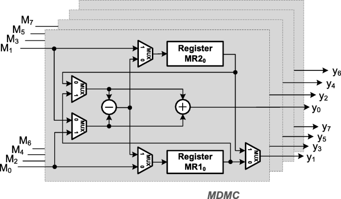
Architecture of the proposed MDMC

2.2.2 Time-allocation scheme
Figure 4 present a flow chart showing the timing of the proposed time allocation scheme, which enables the simultaneous computation of the two dimensions of the transform after the 22th clock cycle, thereby increasing hardware utilization to 100%. In the proposed scheme, the MUX select signals (S1, S2, and S3) to control the switching of the transform among dimensions. The timing of ECSA and OCSA is based on clock cycles in which even and odd part data of the 1st-D (or 2nd-D) of the transform must be computed in ECSA and OCSA modules. MR1n and MR2n (n=0…3) are clock cycles requiring that data be stored in the registers of MDMC. Figure 4 also presents the timing allocation of outputs z2D and y. The allocation of data computation is described in the following.

Time allocation in proposed 2-D IDCT architecture
-
1.
1-D data computation: During the first cycle, the first 1-D even data are fed into pipeline with no input data from the 2-D transform. During the 1st-2nd cycle, the first 1-D odd data are fed into pipeline, and the first 1-D even data stored in the pipeline in the previously cycle are input and computed in the ECSA module, the results of which are stored in registers (MR10,MR11,MR12,MR13) in the MDMC module. During the 2nd-3rd cycle, the first 1-D odd data are fed into the OCSA module and the results are fed into the MDMC to be added to the even data previously stored in the register. Results from the MDMC module are sent to the transpose circuit, and the substrate results are stored in registers (MR10,MR11,MR12,MR13) in the MDMC module. During the 3rd-4th cycle, the computation results of the second even data from ECSA are stored in registers (MR10,MR11,MR12,MR13) and substrate results previously stored in registers are simultaneously fed into the transpose circuit. Thus, the latency associated with the computation of 1-D transform data is 4 clock cycles.
-
2.
2-D data computation: Starting in the 3rd cycle, data from the first dimension of the transform are sent to the transposed circuit. Due to the TMEM in the transposed circuit, transposed 2-D computation data z2D are sent to Reorder 1 during the 22th-23th cycles while the first 2-D even data and 11th 1-D odd data are simultaneously sent to the pipeline. During the 23th-24th cycle, first 2-D odd data shift to the pipeline. The first 2-D even data are sent to ECSA to be computed and the results are stored in registers (MR20,MR21,MR22,MR23) in the MDMC module. At the same time, the 11th 1-D odd data are fed into the OCSA module and results are fed to the MDMC module. During the 24th-25th cycle, 2-D odd data are fed into the OCSA module and added to the even data previously stored in registers (MR20,MR21,MR22,MR23). The addition results are fed to output pots y and the subtraction results are simultaneously stored in registers (MR20,MR21,MR22,MR23) in the MDMC module. During the 25th-26th cycles, the outputs of 2-D IDCT transform y are equal to the subtraction results stored in registers in the MDMC.
-
3.
Hardware utilization: As shown in Fig. 4, between the 1st and 22th cycles, the hardware utilization of the proposed 2-D IDCT core transform core is 50%. After the 22th cycle, hardware utilization increases to 100% with total latency of 26 clock cycles.
In summary, the 1-D IDCT proposed in this study is based on the CSDA algorithm. The proposed method for hardware sharing requires 4 clock cycles for computation using the 1-D IDCT, thereby significantly reducing hardware resource requirements. The proposed time allocation scheme enables the simultaneous calculation of the first and second dimensions of the 1-D IDCT transform following the 22th cycle, thereby achieving hardware utilization of 100%. The result is a high-performance inverse transform engine with high accuracy, low cost, and high throughput.
3 Results and discussion
In this section, we outline the methods used to evaluate the accuracy of the proposed 2-D IDCT core. Then, we compare the proposed 2-D IDCT architecture with existing methods and describe the characteristics of an actual implementation of the proposed chip.
3.1 Accuracy testing of proposed 2-D IDCT core
The MATLAB tool was used to compute the 2-D DCT core transform of the original test image and perform computations, the results of which were used as input data for the proposed 2-D IDCT transform in which we calculated the peak signal-to-noise ratio (PSNR). In accuracy testing for proposed 2-D IDCT core system, we use the images (512 × 512 pixels; 8-bit) to evaluate the accuracy of the 2-D IDCT core system, and the average PSNR is 43.04 dB. PSNR is a quality indicator used to evaluate the quality of image compression. Clearly, the quality of the image decompression is excellent. Figure 5 presents a flowchart illustrating the methods used to verify the accuracy of the proposed 2-D IDCT.

Accuracy verification flow chart of 2-D IDCT illustrating
3.2 Characteristics of chip implementation
The proposed 2-D IDCT core was implemented using RTL hardware based on the TSMC 90 nm standard CMOS process. Following the Synopsys Design Compiler synthesis, the Cadence Encounter digital implementation (EDI) was used for placement and routing (P&R). The proposed 2-D IDCT core has a latency of 26 clock cycles and is capable of being operated at 200 MHz with core area 703×702μm2. The characteristics and the core layout of the test chip with the proposed 2-D IDCT architecture are presented in Fig. 6.

Chip characteristics and layout of proposed video transform
3.3 Comparison to existing works
Table 2 presents a comparison of the proposed and previous methods. In [7], Meher et al. proposed power-efficient structures for folded and full-parallel implementations of 2-D DCT as well as an efficient constant matrix multiplication scheme to derive parallel architectures for 1-D integer DCTs of various lengths used in the HEVC standard. The parallel architecture and two 1-D core with a TMEM requires huge area overhead. The In [8], Fan et al. combined sparse matrix decomposition with shift-and-add computation in a new multiple 1-D fast IDCT in conjunction with hardware sharing. Compared to discrete 1-D hardware, that method reduces hardware costs by 45%. However, two 1-D core with a TMEM consumes large circuit area for applied to the 2-D transform. In [9], Fan et al. adopted sparse matrix decomposition for multiple 1-D and 2-D fast forward/inverse transform algorithms with hardware-sharing, which reduced the gate count by 53.4%. In [13], Lee et al. proposed the novel concept of a delta coefficient matrix in which resources, such as adders and shifters, are combined. In [15], Part et al. proposed a flexible architecture for the transform function, the memory control scheme of which is able to store data for multiple standards. Unlike the works in [7–9, 13], the architecture of this flexible transform core uses only one 1-D IDCT core with a TMEM to save the area cost.
Table 2 provides a comparison of the proposed architecture with previous multiple transform methods. The synthesis results show that the maximum frequency can be increased to 200 MHz, resulting in a maximum data throughput of 800 M-pixels/s when implemented using TSMC 90 nm CMOS standard cell technology. This resulted in a gate count of 27.2 K. Clearly, the proposed 2-D IDCT provides high hardware efficiency, as out-lined in the following:
In summary, the proposed 2-D IDCT architecture provides superior hardware efficiency than that found in existing designs. According to have a fair comparison, the operational frequency can be normalized by the CMOS technology. The delay information for the 180 nm, 130 nm, and 90 nm [16], which are 77.2 ps, 34.7 ps, and 26.5 ps for an inverter delay, is used to normalize the frequency. Thus, the definition of the frequency normalized function is expressed as follows.
where the Freqn indicates the operational frequency normalized to 90 nm technology, and Freqw is the operational frequency that want to be normalized. The Delay90 nm and Delayw are the inverter delay time for the 90 nm and the technology which want to be normalized, respectively. The proposed circuit can also achieve a good hardware efficiency for supporting multiple transform standards.
3.4 Proposed architecture applied to HEVC and future video coding standards
High Efficiency Video Coding (HEVC) is the most recent video coding standard proposed by the ITU-T Video Coding Experts Group and Moving Picture Experts Group [17]. This objective behind this standard is improved compression performance. The proposed hardware sharing architecture accommodates this standard at 8-point dimensions. The synthesis results of architecture including HEVC 8-point dimensions of gate counts and throughput rate are 33.8 K and 800 M-pixels/s, respectively. The even and odd parts of the CSDA algorithm make the transform coefficients possible to meet HEVC standards via hardware sharing. The proposed method can apply to the larger transform size using the row-column decomposition. According to the symmetric property, the N-point DCT/IDCT can be decomposed into even/odd N/2-point DCT/IDCT. The even N/2-point DCT/IDCT can be further decomposed into even/odd N/4-point DCT/IDCT. Thus, the N-point can be decomposed into odd part N/2-, N/4-, …, 8-point DCT/IDCT and even part 8-point DCT/IDCT. The odd part transforms can be implemented using the same method as the proposed OCSA, and the even part can be implemented using the same method as the pro- posed core. This enables the hardware to support a wider range of standards, thereby making it more competitive. The operation of transformation in the video coding always utilizes the symmetric matrix to transfer the image/video to the spectral domain achieving the compression in the spectral domain. Thus, the proposed method can be applied to the existing video coding, such as MPEG 1/2/4, H.264, VC-1, and HEVC, and even recommended to the future video coding (H.266 [18]).
4 Conclusions
This paper presents a cost effective 2-D IDCT for the decoding of MPEG 1/2/4, H.264, and VC-1. The inclusion of a time allocation scheme enables the 1-D inverse transform core to calculate the first and second dimensions using four computation paths simultaneously, thereby achieving 100% hardware utilization. Consequently, the proposed scheme outperforms nearly all previous designs with regard to hardware efficiency support for multiple standards.
Availability of data and materials
Not applicable.
Abbreviations
- 1-D:
-
One-dimensional
- 2-D:
-
Two-dimensional
- 1st-D:
-
First-dimensional
- 2nd-D:
-
Second-dimensional
- CMOS:
-
Complementary Metal-Oxide-Semiconductor
- DA:
-
Distributed arithmetic
- DCT:
-
Discrete cosine transform
- DMC2s:
-
Dual mode computations
- ECSA:
-
Even common sharing distributed arithmetic
- EDI:
-
Encounter digital implementation
- FS:
-
Factor sharing
- HEVC:
-
High Efficiency Video Coding
- IDCT:
-
Inverse discrete cosine transform
- MDMC:
-
Multi-dual mode computation
- OCSA:
-
Odd common sharing distributed arithmetic
- P&R:
-
Placement and routing
- PSNR:
-
Peak signal-to-noise ratio
- TMEM:
-
Transposed memory
- TSMC:
-
Taiwan Semiconductor Manufacturing Company Limited
- VLSI:
-
Very-large-scale integration
References
P Noll, MPEG Digital Audio Coding. IEEE Sig. Process. Mag.14:, 59–81 (1997).
A. Luthra, G. J. Sullivan, T. Wiegand, Introduction to the special issue on the H.264/AVC video coding standard. IEEE Trans. Circ. Syst. Video Technol.13:, 557–559 (2003).
T. Wiegand, G. J. Sullivan, G. Bjntegaard, A. Luthra, Overview of the H.264/AVC video coding standard. IEEE Trans. Circ. Syst. Video Technol.13:, 560–576 (2003).
H. Kalva, J. B. Lee, The VC-1 video coding standard. IEEE Multimed.14:, 88–91 (2007).
C. -P. Fan, G. -A. Su, Fast algorithm and low-cost hardware-sharing design of multiple integer transforms for VC-1. IEEE Trans. Circ. Syst. II Video Technol. 56(10), 788–792 (2009). https://doi.org/10.1109/tcsii.2009.2030366.
Y. H. Chen, R. Y. Jou, C. W. Lui, A high-throughput and area-efficient video transform core with a time division strategy. IEEE Trans. VLSI Syst.22:, 2268–2277 (2014).
P. K. Meher, S. Y. Park, B. K. Mohanty, K. S. Lim, C. Yeo, Efficient integer DCT srchitecture for HEVC. IEEE Tran. Circ. Syst. Video Technol.24:, 168–178 (2014).
C. P. Fan, C. H. Fang, C. W. Chang, S. J. Hsu, Fast multiple inverse transforms with low-cost hardware-sharing design for multi-standard video decoding. IEEE Trans. Circ. Syst. II. 58:, 517–521 (2011).
C. P. Fan, C. W. Chang, S. J. Hsu, Cost effective hardware sharing design of fast algorithm based multiple forward and inverse transforms for H.264/AVC, MPEG-1/2/4, AVS, and VC-1 video encoding and decoding applications. IEEE Tran. Circ. Syst. Video Technol.24(4), 714–720 (2014). https://doi.org/10.1109/tcsvt.2013.2277580.
Y. H. Chen, J. N. Chen, T. Y. Chang, C. W Lu, High-throughput multistandard transform core supporting MPEG/H.264/VC-1 using common sharing distributed arithmetic. IEEE Trans. VLSI Syst.22:, 463–474 (2014).
S. Shen, W. Shen, Y. Fan, X. Zeng, in 2012 IEEE International Conference on Multimedia and Expo. A unified 4/8/16/32-point integer IDCT architecture for multiple video coding standards (IEEE, 2012). https://doi.org/10.1109/icme.2012.7.
Y. C. Chao, H. H. Tsai, Y. H. Lin, J. F. Yang, B. D. Liu, in 2007 IEEE International Conference on Multimedia and Expo. A novel design for computation of all transforms in H.264/AVC decoder (IEEE, 2007). https://doi.org/10.1109/icme.2007.4285050.
S. Lee, K. Cho, Architecture of transform circuit for video decoder supporting multiple standards. Electron. Lett.44:, 274–275 (2008).
W. Hwangbo, C. M. Kyung, A multitransform architecture for H.264/AVC high-profile coders. IEEE Trans. Multimedia. 12:, 157–167 (2010).
J. H. Part, S. H. Lee, K. S. Lim, J. H. Kim, S. Kim, in 2006 IEEE International Symposium on Circuits and Systems. A flexible transform processor architecture for multi-CODECs (JPEG, MPEG-2, 4 and H.264) (IEEE, 2006). https://doi.org/10.1109/iscas.2006.1693841.
A. Stillmaker, B. Baas, Scaling equations for the accurate prediction of CMOS device performance from 180 nm to 7 nm. Integration. 58:, 74–81 (2017).
G. J. Sullivan, J. R. Ohm, W. J. Han, T. Wiegand, Overview of the High Efficiency Video Coding (HEVC) Standard. IEEE Trans. Circ. Syst. Video Technol.22:, 189 (2012).
A. C. Mert, E. Kalali, I. Hamzaoglu, in 2017 IEEE 7th International Conference on Consumer Electronics - Berlin (ICCE-Berlin). An FPGA implementation of future video coding 2D transform (IEEE, 2017). https://doi.org/10.1109/icce-berlin.2017.8210582.
Acknowledgements
The authors would like to thank the National Chip Implementation Center (CIC), Taiwan, for providing the electronic design automation tools.
Funding
This work was supported in part by the Ministry of Science and Technology of Taiwan under project 107-2221-E-182-066 and Chang Gung Memorial Hospital-Linkou under project CMRPD2H0051, CMRPD2G0312, CMRPD2H0301, and CIRPD2F0013.
Author information
Authors and Affiliations
Contributions
Both authors read and approved the final manuscript.
Corresponding author
Ethics declarations
Ethics approval and consent to participate
Not applicable.
Consent for publication
Not applicable.
Competing interests
The authors declare that they have no competing interests.
Additional information
Publisher’s Note
Springer Nature remains neutral with regard to jurisdictional claims in published maps and institutional affiliations.
Rights and permissions
Open Access This article is distributed under the terms of the Creative Commons Attribution 4.0 International License(http://creativecommons.org/licenses/by/4.0/), which permits unrestricted use, distribution, and reproduction in any medium, provided you give appropriate credit to the original author(s) and the source, provide a link to the Creative Commons license, and indicate if changes were made.
About this article

Cite this article
Tseng, YH., Chen, YH. Cost-effective multi-standard video transform core using time-sharing architecture. EURASIP J. Adv. Signal Process. 2019, 49 (2019). https://doi.org/10.1186/s13634-019-0645-1
Received:
Accepted:
Published:
DOI: https://doi.org/10.1186/s13634-019-0645-1